- 您现在的位置:买卖IC网 > Sheet目录488 > NTGS3443T1 (ON Semiconductor)MOSFET P-CH 20V 2.2A 6-TSOP
�� �
�
�NTGS3443,� NVGS3443�
�Power� MOSFET�
�4.4� Amps,� 20� Volts�
�P� ?� Channel� TSOP� ?� 6�
�Features�
�?� Ultra� Low� R� DS(on)�
�?� Higher� Efficiency� Extending� Battery� Life�
�?� Miniature� TSOP� ?� 6� Surface� Mount� Package�
�?� These� Devices� are� Pb� ?� Free� and� are� RoHS� Compliant�
�?� NVGS� Prefix� for� Automotive� and� Other� Applications� Requiring�
�Unique� Site� and� Control� Change� Requirements;� AEC� ?� Q101�
�Qualified� and� PPAP� Capable�
�Applications�
�?� Power� Management� in� Portable� and� Battery� ?� Powered� Products,�
�i.e.:� Cellular� and� Cordless� Telephones,� and� PCMCIA� Cards�
�MAXIMUM� RATINGS� (T� J� =� 25� °� C� unless� otherwise� noted)�
�http://onsemi.com�
�4.4� AMPERES�
�20� VOLTS�
�R� DS(on)� =� 65� m� W�
�P� ?� Channel�
�1� 2� 5� 6�
�3�
�4�
�Rating�
�Drain� ?� to� ?� Source� Voltage�
�Gate� ?� to� ?� Source� Voltage� ?� Continuous�
�Thermal� Resistance�
�Junction� ?� to� ?� Ambient� (Note� 1)�
�Total� Power� Dissipation� @� T� A� =� 25� °� C�
�Drain� Current� ?� Continuous� @� T� A� =� 25� °� C�
�?� Pulsed� Drain� Current� (T� p� t� 10� m� S)�
�Symbol�
�V� DSS�
�V� GS�
�R� q� JA�
�P� d�
�I� D�
�I� DM�
�Value�
�?� 20�
�"� 12�
�244�
�0.5�
�?� 2.2�
�?� 10�
�Unit�
�Volts�
�Volts�
�°� C/W�
�Watts�
�Amps�
�Amps�
�1�
�TSOP� ?� 6�
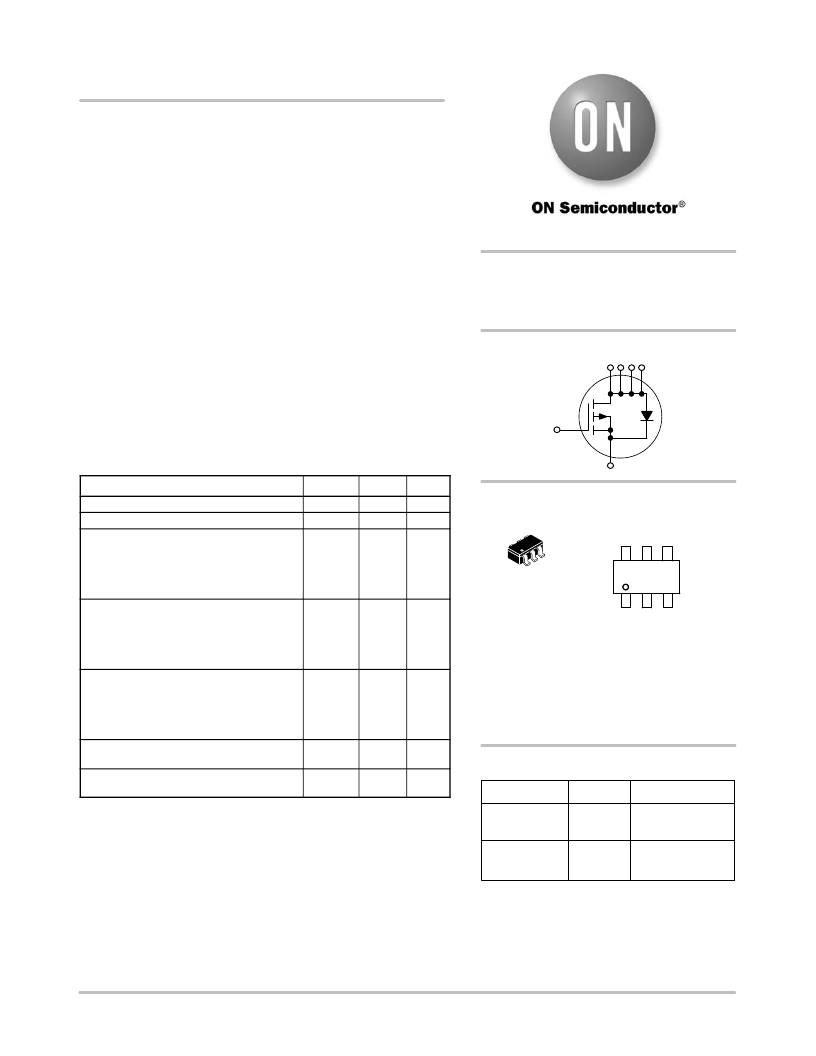
�MARKING� DIAGRAM� &�
�PIN� ASSIGNMENT�
�Drain� Drain� Source�
�6� 5� 4�
�443� M� G�
�G�
�Thermal� Resistance�
�Junction� ?� to� ?� Ambient� (Note� 2)�
�Total� Power� Dissipation� @� T� A� =� 25� °� C�
�Drain� Current� ?� Continuous� @� T� A� =� 25� °� C�
�?� Pulsed� Drain� Current� (T� p� t� 10� m� S)�
�Thermal� Resistance�
�Junction� ?� to� ?� Ambient� (Note� 3)�
�Total� Power� Dissipation� @� T� A� =� 25� °� C�
�Drain� Current� ?� Continuous� @� T� A� =� 25� °� C�
�?� Pulsed� Drain� Current� (T� p� t� 10� m� S)�
�Operating� and� Storage� Temperature� Range�
�Maximum� Lead� Temperature� for� Soldering�
�Purposes� for� 10� Seconds�
�R� q� JA�
�P� d�
�I� D�
�I� DM�
�R� q� JA�
�P� d�
�I� D�
�I� DM�
�T� J� ,� T� stg�
�T� L�
�128�
�1.0�
�?� 3.1�
�?� 14�
�62.5�
�2.0�
�?� 4.4�
�?� 20�
�?� 55� to�
�150�
�260�
�°� C/W�
�Watts�
�Amps�
�Amps�
�°� C/W�
�Watts�
�Amps�
�Amps�
�°� C�
�°� C�
�CASE� 318G�
�STYLE� 1� 1� 2� 3�
�Drain� Drain� Gate�
�443� =� Specific� Device� Code�
�M� =� Date� Code*�
�G� =� Pb� ?� Free� Package�
�(Note:� Microdot� may� be� in� either� location)�
�*Date� Code� orientation� may� vary� depending�
�upon� manufacturing� location.�
�ORDERING� INFORMATION�
�Device� Package� Shipping� ?�
�Stresses� exceeding� Maximum� Ratings� may� damage� the� device.� Maximum�
�Ratings� are� stress� ratings� only.� Functional� operation� above� the� Recommended�
�Operating� Conditions� is� not� implied.� Extended� exposure� to� stresses� above� the�
�Recommended� Operating� Conditions� may� affect� device� reliability.�
�1.� Minimum� FR� ?� 4� or� G� ?� 10� PCB,� operating� to� steady� state.�
�2.� Mounted� onto� a� 2� in� square� FR� ?� 4� board� (1� in� sq,� 2� oz.� Cu.� 0.06� ″� thick� single�
�sided),� operating� to� steady� state.�
�3.� Mounted� onto� a� 2� in� square� FR� ?� 4� board� (1� in� sq,� 2� oz.� Cu.� 0.06� ″� thick� single�
�sided),� t� t� 5.0� seconds.�
�NTGS3443T1G� TSOP� ?� 6� 3000� /� Tape� &� Reel�
�(Pb� ?� Free)�
�NVGS3443T1G� TSOP� ?� 6� 3000� /� Tape� &� Reel�
�(Pb� ?� Free)�
�?For� information� on� tape� and� reel� specifications,�
�including� part� orientation� and� tape� sizes,� please�
�refer� to� our� Tape� and� Reel� Packaging� Specifications�
�Brochure,� BRD8011/D.�
�?� Semiconductor� Components� Industries,� LLC,� 2012�
�December,� 2012� ?� Rev.� 5�
�1�
�Publication� Order� Number:�
�NTGS3443T1/D�
�发布紧急采购,3分钟左右您将得到回复。
相关PDF资料
NTGS3446T1
MOSFET N-CH 20V 2.5A 6-TSOP
NTGS3447PT1G
MOSFET P-CH 12V 3.4A 6-TSOP
NTGS3455T1
MOSFET P-CH 30V 2.5A 6-TSOP
NTGS4111PT2G
MOSFET P-CH 30V 2.6A 6-TSOP
NTGS4141NT1G
MOSFET N-CH 30V 3.5A 6-TSOP
NTGS5120PT1G
MOSFET P-CH 60V 1.8A 6-TSOP
NTHC5513T1
MOSFET N/P-CH 20V 2.1A CHIPFET
NTHD2102PT1G
MOSFET PWR P-CH DUAL 8V CHIPFET
相关代理商/技术参数
NTGS3443T1/D
制造商:未知厂家 制造商全称:未知厂家 功能描述:Power MOSFET 2 Amps, 20 Volts
NTGS3443T1G
功能描述:MOSFET 20V 2A P-Channel RoHS:否 制造商:STMicroelectronics 晶体管极性:N-Channel 汲极/源极击穿电压:650 V 闸/源击穿电压:25 V 漏极连续电流:130 A 电阻汲极/源极 RDS(导通):0.014 Ohms 配置:Single 最大工作温度: 安装风格:Through Hole 封装 / 箱体:Max247 封装:Tube
NTGS3443T1G
制造商:ON Semiconductor 功能描述:MOSFET
NTGS3443T2G
功能描述:MOSFET PFET 20V 0.10R TR RoHS:否 制造商:STMicroelectronics 晶体管极性:N-Channel 汲极/源极击穿电压:650 V 闸/源击穿电压:25 V 漏极连续电流:130 A 电阻汲极/源极 RDS(导通):0.014 Ohms 配置:Single 最大工作温度: 安装风格:Through Hole 封装 / 箱体:Max247 封装:Tube
NTGS3446
制造商:ONSEMI 制造商全称:ON Semiconductor 功能描述:Power MOSFET 5.1 Amps, 20 Volts N−Channel TSOP−6
NTGS3446/D
制造商:未知厂家 制造商全称:未知厂家 功能描述:Power MOSFET 5 Amps, 20 Volts
NTGS3446T1
功能描述:MOSFET 20V 5.1A N-Channel RoHS:否 制造商:STMicroelectronics 晶体管极性:N-Channel 汲极/源极击穿电压:650 V 闸/源击穿电压:25 V 漏极连续电流:130 A 电阻汲极/源极 RDS(导通):0.014 Ohms 配置:Single 最大工作温度: 安装风格:Through Hole 封装 / 箱体:Max247 封装:Tube
NTGS3446T1G
功能描述:MOSFET 20V 5.1A N-Channel RoHS:否 制造商:STMicroelectronics 晶体管极性:N-Channel 汲极/源极击穿电压:650 V 闸/源击穿电压:25 V 漏极连续电流:130 A 电阻汲极/源极 RDS(导通):0.014 Ohms 配置:Single 最大工作温度: 安装风格:Through Hole 封装 / 箱体:Max247 封装:Tube